- 您现在的位置:买卖IC网 > Sheet目录512 > SI7100DN-T1-GE3 (Vishay Siliconix)MOSFET N-CH D-S 8V PPAK 1212-8
�� �
�
�Si7100DN�
�Vishay� Siliconix�
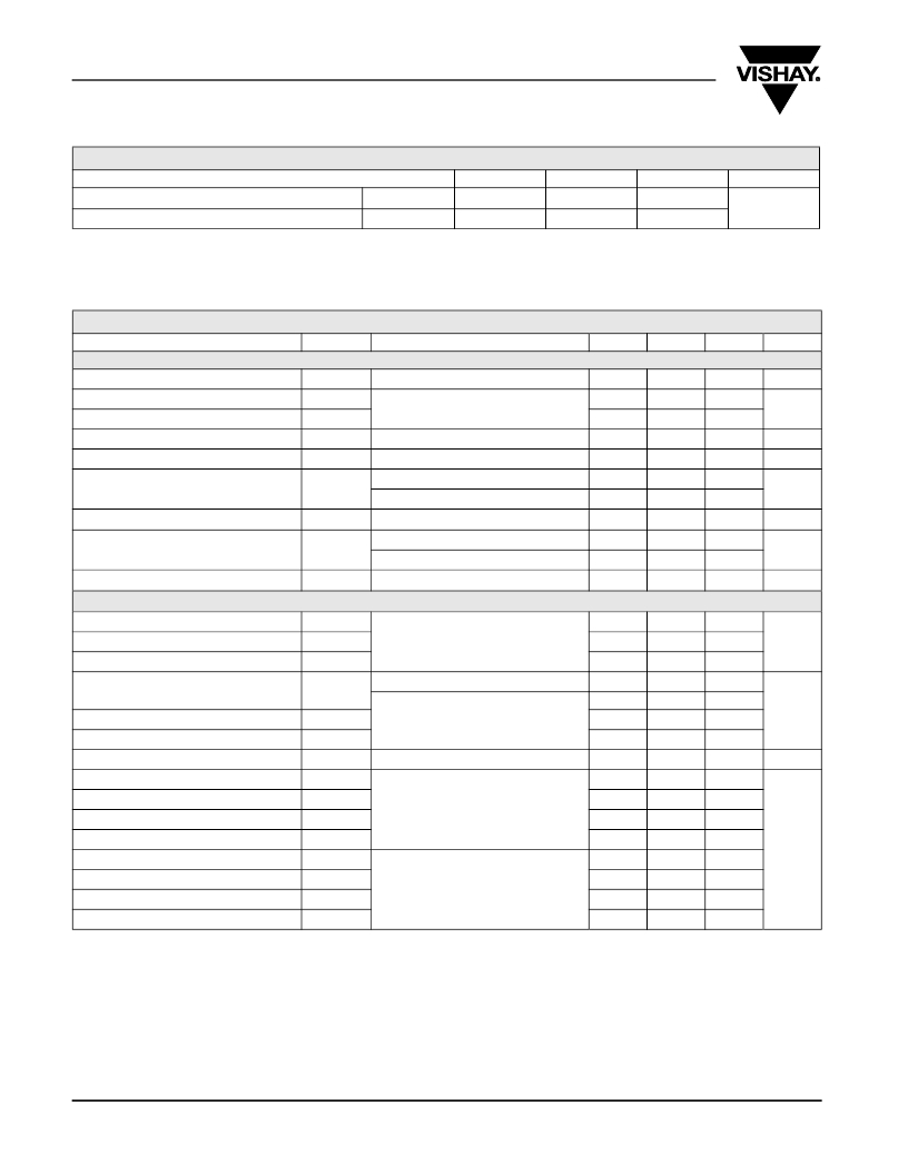
�THERMAL� RESISTANCE� RATINGS�
�Parameter�
�Symbol�
�Typical�
�Maximum�
�Unit�
�Maximum� Junction-to-Ambient�
�a,� b�
�Maximum� Junction-to-Case� (Drain)�
�t� ≤� 10� s�
�Steady� State�
�R� thJA�
�R� thJC�
�24�
�1.9�
�33�
�2.4�
�°C/W�
�Notes:�
�a.� Surface� Mounted� on� 1"� x� 1"� FR4� board.�
�b.� Maximum� under� Steady� State� conditions� is� 81� °C/W.�
�SPECIFICATIONS� T� J� =� 25� °C,� unless� otherwise� noted�
�Parameter�
�Symbol�
�Test� Conditions�
�Min.�
�Typ.�
�Max.�
�Unit�
�Static�
�Drain-Source� Breakdown� Voltage�
�V� DS� Temperature� Coefficient�
�V� GS(th)� Temperature� Coefficient�
�V� DS�
�Δ� V� DS� /T� J�
�Δ� V� GS(th)� /T� J�
�V� GS� =� 0� V,� I� D� =� 250� μA�
�I� D� =� 250� μA�
�8�
�12�
�-� 3.5�
�V�
�mV/°C�
�Gate-Source� Threshold� Voltage�
�V� GS(th)�
�V� DS� =� V� GS� ,� I� D� =� 250� μA�
�0.4�
�1.0�
�V�
�Gate-Source� Leakage�
�Zero� Gate� Voltage� Drain� Current�
�On-State� Drain� Current� a�
�I� GSS�
�I� DSS�
�I� D(on)�
�V� DS� =� 0� V,� V� GS� =� ±� 8� V�
�V� DS� =� 8� V,� V� GS� =� 0� V�
�V� DS� =� 8� V,� V� GS� =� 0� V,� T� J� =� 55� °C�
�V� DS� ≥� 5� V,� V� GS� =� 4.5� V�
�30�
�±� 100�
�1�
�10�
�nA�
�μA�
�A�
�Drain-Source� On-State� Resistance� a�
�Forward� Transconductance� a�
�R� DS(on)�
�g� fs�
�V� GS� =� 4.5� V,� I� D� =� 15� A�
�V� GS� =� 2.5� V,� I� D� =� 10� A�
�V� DS� =� 5� V,� I� D� =� 15� A�
�0.0029�
�0.0035�
�120�
�0.0035�
�0.0045�
�Ω�
�S�
�Dynamic� b�
�Input� Capacitance�
�C� iss�
�3810�
�Output� Capacitance�
�Reverse� Transfer� Capacitance�
�C� oss�
�C� rss�
�V� DS� =� 4� V,� V� GS� =� 0� V,� f� =� 1� MHz�
�1625�
�1205�
�pF�
�Total� Gate� Charge�
�Gate-Source� Charge�
�Q� g�
�Q� gs�
�V� DS� =� 4� V,� V� GS� =� 8� V,� I� D� =� 10� A�
�V� DS� =� 4� V,� V� GS� =� 4.5� V,� I� D� =� 10� A�
�69�
�40�
�3.8�
�105�
�60�
�nC�
�Gate-Drain� Charge�
�Q� gd�
�8.2�
�Gate� Resistance�
�Turn-On� Delay� Time�
�Rise� Time�
�Turn-Off� Delay� Time�
�Fall� Time�
�Turn-On� Delay� Time�
�Rise� Time�
�Turn-Off� Delay� Time�
�Fall� Time�
�R� g�
�t� d(on)�
�t� r�
�t� d(off)�
�t� f�
�t� d(on)�
�t� r�
�t� d(off)�
�t� f�
�f� =� 1� MHz�
�V� DD� =� 4� V,� R� L� =� 0.8� Ω�
�I� D� ?� 5� A,� V� GEN� =� 4.5� V,� R� g� =� 1� Ω�
�V� DD� =� 4� V,� R� L� =� 0.8� Ω�
�I� D� ?� 5� A,� V� GEN� =� 8� V,� R� g� =� 1� Ω�
�1.1�
�19�
�57�
�61�
�10�
�14�
�52�
�53�
�8�
�1.7�
�30�
�90�
�95�
�15�
�25�
�80�
�80�
�15�
�Ω�
�ns�
�www.vishay.com�
�2�
�Document� Number:� 73785�
�S-80581-Rev.� C,� 17-Mar-08�
�发布紧急采购,3分钟左右您将得到回复。
相关PDF资料
SI7107DN-T1-GE3
MOSFET P-CH 20V 9.8A 1212-8
SI7110DN-T1-GE3
MOSFET N-CH 20V 13.5A 1212-8
SI7115DN-T1-E3
MOSFET P-CH D-S 150V PPAK 1212-8
SI7120DN-T1-GE3
MOSFET N-CH 60V 6.3A 1212-8
SI7123DN-T1-GE3
MOSFET P-CH 20V 10.2A 1212-8
SI7129DN-T1-GE3
MOSFET P-CH D-S 30V 1212-8
SI7135DP-T1-GE3
MOSFET P-CH 30V 60A PPAK 8SOIC
SI7136DP-T1-GE3
MOSFET N-CH 20V 30A PPAK 8SOIC
相关代理商/技术参数
SI-71011-F
制造商:BEL 制造商全称:Bel Fuse Inc. 功能描述:SI-71011-F
SI7101DN-T1-GE3
功能描述:MOSFET -30V 7.2mOhm@10V -35A P-Ch G-III
RoHS:否 制造商:Vishay Semiconductors 晶体管极性:P-Channel 汲极/源极击穿电压:- 30 V 闸/源击穿电压:25 V 漏极连续电流:- 35 A 电阻汲极/源极 RDS(导通):0.0072 Ohms 配置:Dual Dual Drain 最大工作温度:+ 150 C 安装风格:SMD/SMT 封装 / 箱体:PowerPak-1212-8 封装:Reel
SI7102DN
制造商:VISHAY 制造商全称:Vishay Siliconix 功能描述:N-Channel 12-V (D-S) MOSFET
SI7102DN-T1-E3
功能描述:MOSFET 12V 35A 52W RoHS:否 制造商:STMicroelectronics 晶体管极性:N-Channel 汲极/源极击穿电压:650 V 闸/源击穿电压:25 V 漏极连续电流:130 A 电阻汲极/源极 RDS(导通):0.014 Ohms 配置:Single 最大工作温度: 安装风格:Through Hole 封装 / 箱体:Max247 封装:Tube
SI7102DN-T1-GE3
功能描述:MOSFET 12V 35A 52W 3.8mohm @ 4.5V RoHS:否 制造商:STMicroelectronics 晶体管极性:N-Channel 汲极/源极击穿电压:650 V 闸/源击穿电压:25 V 漏极连续电流:130 A 电阻汲极/源极 RDS(导通):0.014 Ohms 配置:Single 最大工作温度: 安装风格:Through Hole 封装 / 箱体:Max247 封装:Tube
SI7104DN-T1-E3
功能描述:MOSFET 12V 35A RoHS:否 制造商:STMicroelectronics 晶体管极性:N-Channel 汲极/源极击穿电压:650 V 闸/源击穿电压:25 V 漏极连续电流:130 A 电阻汲极/源极 RDS(导通):0.014 Ohms 配置:Single 最大工作温度: 安装风格:Through Hole 封装 / 箱体:Max247 封装:Tube
SI7104DN-T1-GE3
功能描述:MOSFET 12V 35A 52W 3.7mohm @ 4.5V RoHS:否 制造商:STMicroelectronics 晶体管极性:N-Channel 汲极/源极击穿电压:650 V 闸/源击穿电压:25 V 漏极连续电流:130 A 电阻汲极/源极 RDS(导通):0.014 Ohms 配置:Single 最大工作温度: 安装风格:Through Hole 封装 / 箱体:Max247 封装:Tube
SI7106DN
制造商:VISHAY 制造商全称:Vishay Siliconix 功能描述:N-Channel 20-V (D-S) Fast Switching MOSFET